


Inventory | 2018 Top Ten Optical Industry Technologies
After reviewing 13,659 related news from major optical media platforms, and asking industry experts, as well as our year-round inspection of the optoelectronic industry in 2018, ten technologies that have a positive impact on the development of the industry have been selected. Promote industrial processes in their respective fields.
What are the top ten technologies, follow us one by one.
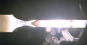
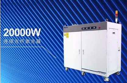
Domestic 20kW high-power all-fiber laser put into production
In recent years, fiber lasers have become more and more widely used in industrial markets, but high-power markets are basically controlled by foreign companies. In 2016, the major task of Hubei Province’s technological innovation special project “R & D of 20 kW fiber laser and its core devices” rested on the shoulder of Ruike Laser. After more than two years of hard work, this project passed the expert acceptance organized by the Science and Technology Department of Hubei Province on October 17, 2018.
This project realized the development of a 20 kW all-fiber laser for the first time in China, filling a domestic gap and breaking the monopoly of a small number of foreign manufacturers on this product. It has mastered the core technology of fiber lasers, and realized high-power fiber lasers and their key points The localization of devices and the development of mid- to high-end fiber laser industry are of great significance.
The 20 kW all-fiber laser has started small-scale production.
China’s first commercial 100G silicon optical chip officially put into production
China’s first commercial 100G silicon optical chip was officially put into production. This commercial silicon optical chip integrates nearly 60 active and passive optical components including light transmission, modulation, and reception on a silicon chip of less than 30 square millimeters. When the chip is packaged, the size of its silicon optical device product is only 312 square millimeters, and its area is only one-third that of traditional devices.
The chip was jointly developed by the National Information Optoelectronics Innovation Center, Optics Technology Co., Ltd., the State Key Laboratory of Optical Fiber Communication Technology and Networks, and China Information and Communication Technology Group. Production, and passed the user’s live network test, the performance is stable and reliable.
The world’s first iris recognition ASIC chip successfully taped out
After 7 years of technical research, QX8001, the world’s first iris biometric ASIC chip developed by Wuhan Hongshi Technology Co., Ltd., was successfully taped out. It passed an rigorous function and performance test and completed an important step before mass production.
The QX8001 chip uses a 40 nm semiconductor manufacturing process, with an average power consumption of only 0.1 W. It can process 1920 × 1080 pixel high-definition images with an image encoding speed of 100 ms. The iris recognition accuracy is higher than previous iris recognition technologies.
In the future, this chip can be integrated by general smart terminal equipment manufacturers such as smart watches, smart phones, smart door locks, and smart access control as general applications such as login, startup, encryption, payment, and door opening.It can also be used by iris collectors, police, The integration of specialized terminal equipment manufacturers such as customs clearance gate knives enables special applications such as iris biometric database construction, black-and-white list lookup, border and immigration control.
After the chip is mass-produced, it can solve the problems of expensive, large volume and high power consumption of iris biometric identification equipment, and make the iris biometric technology and products widely used.
4m large-aperture silicon carbide aspheric optical reflector successfully developed
Large-caliber high-precision aspheric optical mirrors are the core components of high-resolution space-to-ground observation, deep-space exploration, and astronomical observation systems. Their manufacturing technology level is of great significance to national defense security, national economic construction, and basic scientific research capabilities. As a kind of high-stability optical mirror material, in the past quite a long time, the maximum diameter of the monomer silicon carbide mirror publicly reported internationally was only 1.5 meters.
Zhang Xuejun, deputy director of the Changchun Institute of Optics and Mechanics of the Chinese Academy of Sciences, led the team to break through a number of key blank preparation technologies, established a large-caliber silicon carbide mirror blank manufacturing platform, and successively developed 2m, 2.4m, and 3m single sheets that can be used for visible light imaging Bulk silicon carbide mirror blank and 4 meter caliber monolithic silicon carbide mirror blank. At the same time, they also overcome two other technical bottlenecks-large-aperture silicon carbide aspheric processing testing and high-performance modification and coating, forming a large-aperture series of mirror development capabilities, which is a major technology in the field of large-aperture optical manufacturing in China. breakthrough.
High-performance streak camera developed successfully, breaking international monopoly
People are not unfamiliar with the “microscopy” technology. This is a spatial magnification technique for observing the microworld, which can “extend” the spatial resolution of the human eye, while ultra-high-speed imaging is a time magnification technique for observing transient events. “The time resolution of the human eye. The streak camera is the necessary means to realize this microscopic and ultra-fast process detection. It is also the only high-end scientific measurement and diagnostic instrument with both ultra-high time resolution and high spatial resolution. It is also indispensable in the national strategic high-tech research of inertial confinement laser fusion. Or missing diagnostic equipment.
As a very sensitive cutting-edge technology, the international academic research results of streak cameras and the sharing of devices and equipment are very low. Foreign related technologies have imposed strict blockades on China, and strict export controls have also been imposed on streak cameras. The Chinese Academy of Sciences Xi’an Opto-Mechanical Research Institute has established the only streak camera research and development base in China that integrates design, production and testing. At present, eight types of streak cameras have been successfully developed.
On May 22, 2018, the National Key Scientific Research Equipment Project “Development of High-Performance Stripe Cameras” undertaken by Xi’an Opto-Mechanics of the Chinese Academy of Sciences successfully passed the acceptance test, marking that China’s high-performance stripe cameras with independent intellectual property rights have reached the practical level. This achievement breaks the international monopoly in this field and is of great significance to cutting-edge scientific research and major national engineering construction.
The world’s largest optical quantum computing chip is launched
Each of the twenty photon arrays in the chip shown contains 2401 waveguides
In May 2018, Science Advances reported the latest research results of Jin Xianmin’s research team in the School of Physics and Astronomy of Shanghai Jiaotong University-the world’s largest three-dimensional integrated optical quantum chip, and demonstrated the first real two-dimensional random walk quantum computing . At the same time, this is also the first optical quantum computing chip in China. This research progress is of great significance for advancing the research of analog quantum computers.
Quantum information technology has gone through extensive theoretical verifications. Whether it can really get out of the laboratory and move towards practicality and industrialization depends on whether we can build and manipulate a sufficiently large-scale quantum system. The development of optical quantum integrated chip technology is a promising way to overcome the scalability problem, and it is expected to strongly promote the substantial progress of quantum information technology.
6000 W nanosecond pulsed laser pushes for industrial application
On January 8th, at the 2017 National Science and Technology Awards Conference held in Beijing, the “Research on Deep-level Doping Mechanisms of New Semiconductors” project of Professor Li Jingbo, Chairman of China Science and Technology Spectrum Laser Technology Co., Ltd. won the second prize of National Natural Science Award prize.
Supported by research on scientific issues such as semiconductor laser epitaxial growth and doping technology, Li Jingbo’s team has recently achieved a number of innovations in key technologies for high-power semiconductor laser chips: the development of nanosecond pulse lasers with an average power of 6000 W. It is 2000 W higher than the current similar indicators in the world. The first development of a high-power semiconductor laser chip has a single-bar power of more than 160 W and a lifetime of more than 10,000 hours.
Field experiment with laser puncture
The Li Jingbo team has successfully converted some of the achievements of this award-winning project into the industrial application of high-power pulsed lasers, and founded Nanchang Zhongke Chuangpu Laser Technology Co., Ltd. It is expected that the company’s sales revenue will exceed 100 million yuan in 2018.
New quantum dot display materials and devices successfully developed
Hefei University of Technology researchers cooperated with the University of Science and Technology of China and the Guangdong Academy of Sciences to successfully apply graphite phase carbon nitride to the next-generation quantum dot display (QLED) technology for the first time, and successfully prepared a new type of quantum dot display device.
QLED has the advantages of high color purity, wide color gamut, easy to realize large-screen flexible display, and low device cost. It is considered to be the next-generation display technology after OLED, but it is urgent to develop new materials and new devices to realize this technology.
Researchers synthesized a carbonitride powder with a graphene-like two-dimensional sheet structure by thermal polymerization, and then prepared quantum dots by ultrasonic stripping technology. Using the quantum dots as a light-emitting layer, they were prepared by the solution spin coating method. Blue glowing quantum dots show the prototype device. Experiments show that the luminous efficiency of this quantum dot material can reach 49.8%.
This achievement has opened up new research directions for the next generation of quantum dot display technology. At present, researchers are optimizing and improving the luminous brightness, luminous efficiency, color purity, and color saturation of this new material to meet the application requirements of the new display industry. .
High-precision microwave photon imaging radar
Professor Pan Shilong’s group of Nanjing University of Aeronautics and Astronautics has jointly developed the Broadband Microwave Photon Imaging Radar with the Intelligent Perception Laboratory of the 14th Research Institute of China Electronics Technology Group. This technology overcomes the two major technical problems of broadband signal generation and broadband real-time imaging processing. Not only can it obtain an image with an imaging resolution better than 1.3 cm × 1.3 cm, it can also observe small-sized targets with high accuracy in the form of video.
In addition to the wide application of this technology in intelligent devices such as autonomous vehicles, drones, and autonomous robots, the technology has obtained a technical foundation, and high-precision real-time video microwave imaging also has advantages for individual soldiers, combat vehicles and helicopters in counterterrorism operations in complex environments Extremely important.
Changguang Huaxin 976 nm Pumped Fiber Laser
Changguang Huaxin’s high-brightness 976 nm fiber-coupled semiconductor laser uses an independently matured 976 nm single-tube chip, and achieves 135 μm fiber output 160 W 976 nm laser through multiple single-tube series technology, reasonable thermodynamic design and reliable packaging process . A large number of deliveries to the market over the years have truly realized the “Made in China” of semiconductor lasers, which is one of the ideal choices for high-power fiber laser pumping sources.
In addition, the 976 nm pumped fiber laser achieves nearly 85% light-to-light conversion efficiency due to the elimination of fiber nonlinear effects, and the entire system is slightly affected by ambient temperature.