


Correlation between laser surface processing and laser marking
In the past few decades, the laser marking industry has achieved remarkable development. Nowadays, there are a large number of laser marking system suppliers serving various industries around the world. The most important change in this market is the introduction of low-power pulsed fiber lasers, which has now grown to the point that almost every supplier can provide this type of fiber laser marking equipment within its product supply range. The wavelength of these lasers usually belongs to the near-infrared (NIR) category around 1070nm, which is very suitable for marking of most metal products, because the reflectivity of this wavelength is lower than that of CO2 laser with longer wavelength.
But even in this wavelength range, the difficulty of marking different metals is not the same. Aluminum, copper and its alloys are widely used in almost every industry. These materials can be marked with lasers, but it is still difficult to mark the dark-colored marks clearly visible to the naked eye under low heat conditions. In addition, a proven technology has shown that highly transmissive materials can often be processed with marking and micro-modeling with minimal damage within pulse widths that are not associated with unexpected non-linear characteristics.
Laser surface processing
In the broad field of industrial laser material processing, the term laser surface processing is often used to describe a series of processing activities using continuous wave (CW) near-infrared laser sources with a power of several kilowatts. However, the above process is completely different from the techniques described herein that can be considered as micro and nano-scale surface applications. Many of these processes have been developed using short-pulse picosecond (10-12) and femtosecond (10-15) ultrafast lasers, and many articles have been published on how to modify the surface of non-thermal mechanisms.
The main disadvantage of these processes is that even if they belong to the low-power series in this laser category, their investment and operating costs are still high. Because the processing speed usually depends on the average power of the laser, for most industrial laser users, the cost of laser processing under actual surface coverage conditions may be too high. Recently, the range of mature nanosecond-pulse fiber lasers has been extended to the sub-nanosecond range, with the concomitant increase in peak power capabilities by orders of magnitude. Therefore, it is possible to develop a new laser surface processing process using a cost-effective long picosecond laser source.
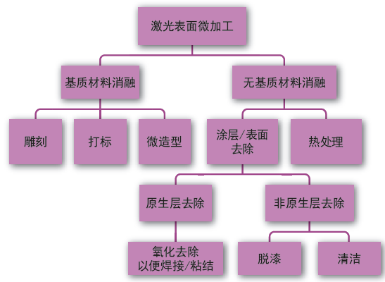
Figure 1: A series of laser surface treatment processes at different levels based on widely accepted terms in the industry and the main physical mechanisms involved.
Although these techniques are often referred to as laser micro-sculpting, from a mechanical point of view, these processes are closely related to laser marking because they are limited to the surface treatment of parts and often require a combination of laser ablation and melting processes. Figure 1 attempts to classify this wide range of processes using industry-accepted terminology and the main physical mechanisms involved.
Near-infrared fiber lasers The
widely known advantages of fiber lasers ensure that they become the dominant near-infrared laser light source option in most applications shown in Figure 1. Of course, the pulsed fiber laser source, with its high average power (up to 4kW), has opened up applications for laser cleaning and laser stripping. The new fiber laser used here has a pulse duration ranging from 0.15 to 5 ns, a peak power of 0.5 mW, a brightness per square meter of <2, and a pulse repetition rate of more than 1 MHz at an average power of up to 30 W. The purpose of this article is to improve the understanding of the function of micron-level lasers, which are used to micro-shape or mark the surface of materials that are generally considered difficult to mark with standard infrared wavelengths, such as copper and glass.
Laser micromodeling and laser marking analysis
By changing the laser marking surface area in a certain way to make it a visual contrast with the unmarked area, this makes laser marking useful. Not only some early results are listed here, but also advanced analysis methods are used to perform in-depth characterization and characterization of laser micro-molding processes on metal and glass surfaces.
The pen-type surface profiler is perhaps the most famous and widely used technique for quantifying surface topography. Therefore, this technique was selected for preliminary evaluation of laser processing. Surface morphology is a qualitative and quantitative description of more general surface characteristics and shapes, and imaging techniques are more useful here. Therefore, two-dimensional and three-dimensional images of the confocal laser scanning microscope were selected.
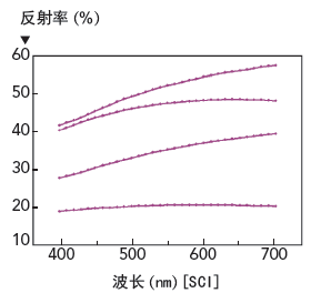
Figure 2: Reflection effect of bare aluminum material processed with a high peak power, sub-nanosecond fiber laser.
Advanced spectrophotometers are widely used to quantify surface color. This can be achieved by analyzing the reflected light from multiple points on the visible spectrum. Regardless of whether or not specular elements are included, unique reflection curves reflecting the characteristics of each surface can be formed. These instruments are also widely used to measure the surface L * value or the color depth of a surface. This technology is now an indispensable tool for quantifying the marking effect of lasers on various consumer products. These reflection curves and L * values were used to quantify the effectiveness of high peak power, short-pulse fiber lasers (Figure 2) on three challenging materials, aluminum, copper, and glass.
Laser surface treatment or micro-modeling
of aluminum. For aluminum materials, its natural oxide layer is hygroscopic and its thickness will increase over time. Therefore, removing this rough and contaminated oxide layer to expose the underlying aluminum material may be sufficient to form sufficient contrast. Another more complicated factor is that the degree of melting or ablation of the underlying aluminum material can significantly affect the appearance of the mark. Careful adjustment of the parameters of the laser can produce a brighter surface to exhibit the fusion effect with increased contrast. By using a pulse energy of ~ 1mJ, it is possible to form a deep color and high oxidation surface on aluminum. However, if you want to obtain a low L * value, you can also obtain a solid, non-fragile surface So that the appearance of the mark does not change with the change of the viewing angle, careful control of the process is required. Increasing the ablation level to form a slightly roughened surface can also obtain a surface with darker color, higher absorption, and a larger L * value (Figure 3). The surface sizes shown are all <10μm, and the surface roughness (Ra) is much lower than <5μm.
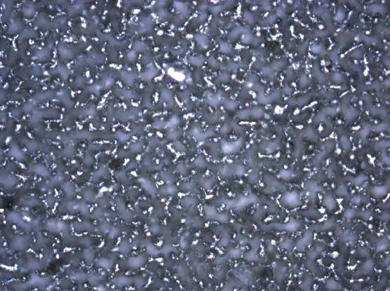
Figure 3: Dark gray aluminum surface treated with a 5ns, 75μJ laser, magnification: 200X.
The removal of anodized coatings from aluminum surfaces is a widely used technique, and the same rules apply to applying lasers to substrates-strong melting means a more reflective surface. No matter it is bare aluminum or anodized aluminum, the marking speed reaches a high level of 1-2m / s. Recently, laser marking technology on specific anodized coatings has been developed. Using low nanosecond and subnanosecond fiber lasers can achieve L * values of <30, although the marking speed is much lower than the above method.
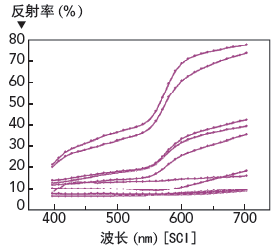
Figure 4: Surface effect of 0.8 mm thick copper material treated with 0.15 nanosecond and 1 nanosecond pulses.
Laser micromodeling or marking of copper materials
Laser-polishing copper materials for contrast is a relatively well-known method, but because of the inherent high reflectivity of this metal, it is often more difficult to obtain dark markings. IPG Photonics’ Silicon Valley Technology Center (SVTC) has developed this type of technology to produce a dark surface with an L * value of <30 on the surface of copper materials. As shown in Figure 5, by comparing with the surface roughness before polishing, it can be seen that the difference in roughness of the laser-treated surface (<1 μmRa). However, the surface structure is more complicated, and the surface area is greatly improved, resulting in a highly absorbent surface. This can be seen from Figure 4.
The rightmost part of FIG. 5 is the polishing area without laser treatment, and the left side is the laser treated area. These features are an order of magnitude smaller than those formed on aluminum materials (Figure 3). The obtained surface structure supports the hypothesis of a non-linear, plasma-controlled process, rather than the traditional heat removal process. Further relevant evidence is that the same laser parameters can be used to process 20 μm-thick copper foil without causing material deformation, although a sub-nanosecond laser with an average power of 28.5W is used.
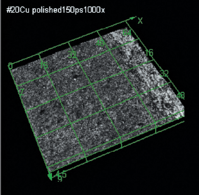
Figure 5: Copper material treated with 150 picosecond pulses.
Laser micromodeling or marking of glass
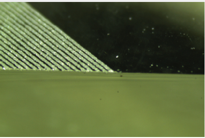
Unexpectedly, almost the same parameters as those used for copper materials can also be applied to the marking of the upper and lower surfaces of uncoated borosilicate glass. This further supports the hypothesis that non-linear absorption is due to the influence of high-peak-power fiber lasers. Checking the scribe area, you can see that the “cracking” condition is very limited, with cracks <10μm and surface roughness <5μmRa. Figure 6 shows the underlined and non-cracked condition under a low magnification.
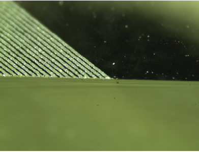
Figure 6: Scribing and non-cracking conditions on the treated copper material under low magnification.
The most interesting results of this process are shown in Figure 7. Among them, the reflectivity of the glass surface can be tightly controlled by changing the scanning parameters.
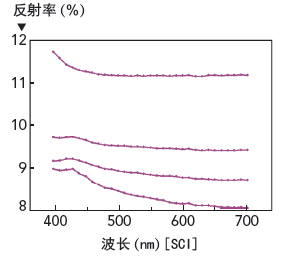
Figure 7: Effect of uncoated borosilicate glass treated with a 150 picosecond laser at a scan speed of 1–1.5 m / s.
Discussion and Summary
We explored how to quantify laser marking and micro-styling and use these techniques to laser mark aluminum. We have also developed technology for marking more challenging copper and uncoated glass surfaces, which clearly shows that there will be process applications for a wider range of surface structures in the future.
Laser welding between copper or other metals has always been a problem in the field of low-power heat conduction welding, because of the inherent high reflectivity and diffusion coefficient, and the inconsistent native surface oxide layer. It turns out that this dark marking technology can improve consistency when welding copper. As part of ongoing research to improve and regulate surface absorptivity through laser beams, these fine structures can also improve the bond between copper or aluminum and other dissimilar metals.
In the relevant case, the same sub-nanosecond laser was used to laser pretreat the metal so that it could later adhere to the transmissive polymer. The advantages of laser-cleaned surfaces, such as increased surface area due to laser pretreatment and local laser heating, facilitate the combination of specific metal-polymer combinations to easily reach the strength level of the substrate.
Finally, the ability to diffuse or scatter light on optical surfaces using conventional laser scanning techniques is guaranteed. The application under consideration is to control glare, which in turn makes processed objects more visible to the human eye. The advent of the significantly enhanced and cost-effective fiber lasers shown here enables customers to shift laser marking from low-cost applications to higher value-added marking and micro-modeling applications.